- 您现在的位置:买卖IC网 > Sheet目录1902 > AT32UC3C2512C-A2UT (Atmel)IC MCU AVR32 512K FLASH 64TQFP
69
32117DS–AVR-01/12
AT32UC3C
7.8.8
Analog Comparator Characteristics
Note:
1. The measures are done without any I/O activity on VDDANA/GNDANA power domain.
7.8.9
USB Transceiver Characteristics
7.8.9.1
Electrical Characteristics
The USB on-chip buffers comply with the Universal Serial Bus (USB) v2.0 standard. All AC
parameters related to these buffers can be found within the USB 2.0 electrical specifications.
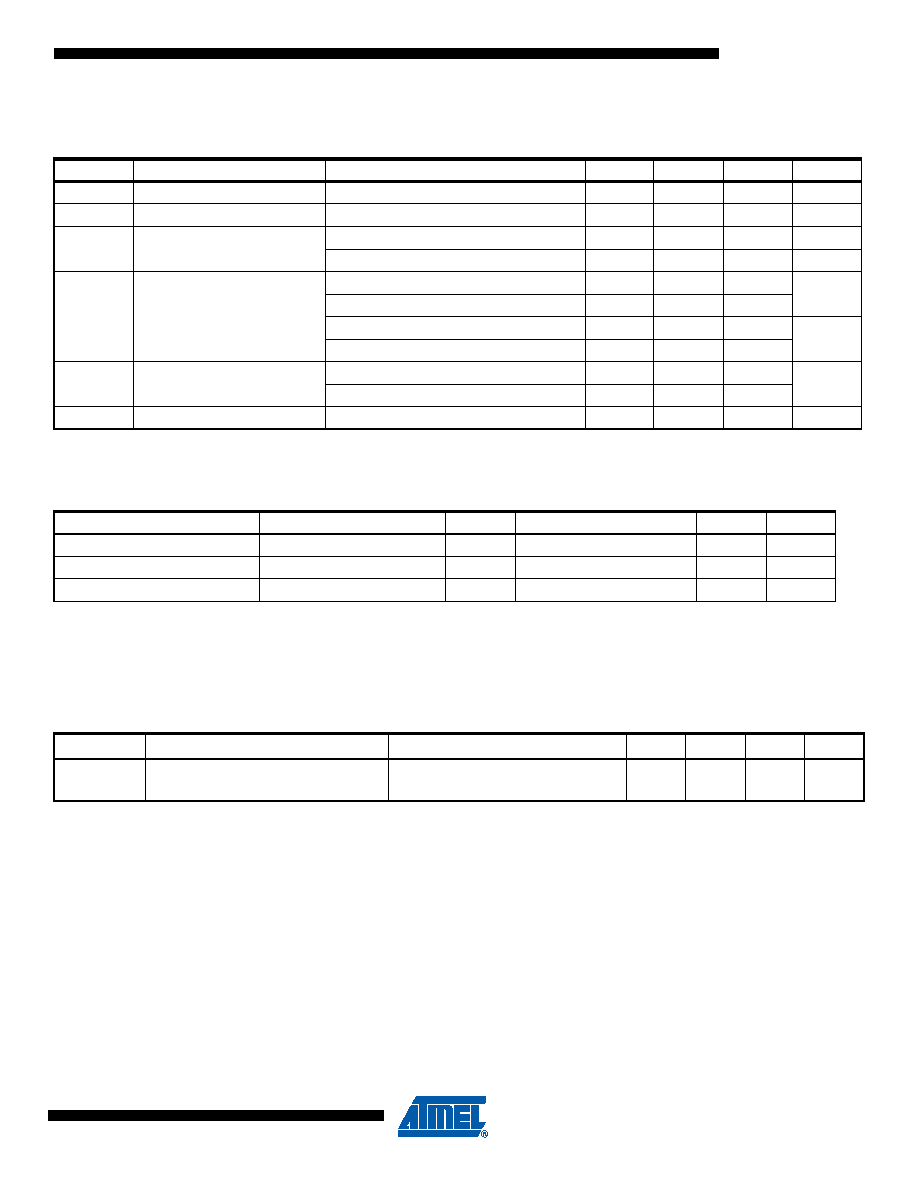
Table 7-41.
Analog Comparator Characteristics(1)
Symbol
Parameter
Conditions
Min
Typ
Max
Units
Positive input voltage range
0
V
VDDANA
V
Negative input voltage range
0
V
VDDANA
V
OFFSET
Offset
No hysteresis, Low Power mode
-29
29
mV
No hysteresis, High Speed mode
-16
16
mV
V
HYST
Hysteresis
Low hysteresis, Low Power mode
7
44
mV
Low hysteresis, High Speed mode
5
34
High hysteresis, Low Power mode
16
102
mV
High hysteresis, High Speed mode
12
69
t
DELAY
Propagation delay
Low Power mode
2.9
us
High Speed mode
0.096
t
STARTUP
Start-up time
20
s
Table 7-42.
VDDANA scaled reference
Symbol
Parameter
Min
Typ
Max
Units
SCF
ACIFA.SCFi.SCF range
0
32
VVDDANA scaled
(64 - SCF) * VVDDANA / 65
V
VDDANA voltage accuracy
3.2
%
Table 7-43.
Electrical Parameters
Symbol
Parameter
Conditions
Min.
Typ.
Max.
Unit
R
EXT
Recommended external USB series
resistor
In series with each USB pin with
±5%
39
Ω
发布紧急采购,3分钟左右您将得到回复。
相关PDF资料
AT32UC3C2512C-A2ZT
IC MCU 32BIT 512KB FLASH 64TQFP
AT32UC3L016-D3HR
MCU AVR32 16K FLASH 48TTLGA
AT42QT5480-CU QS444
IC SENSOR DUAL TOUCH 49-BGA
AT6010H-4QI
IC FPGA 4NS 240PQFP
AT80C31X2-SLRUM
MCU ROMLESS 31X2 5V 44-PLCC
AT80C51RD2-SLRUM
IC MCU 80C51 HI PERFORM 44PLCC
AT85C51SND3B1-RTTUL
IC DECODER/ENCODER DGTL 100-LQFP
AT87251G2D-RLTUM
IC MCU 8/16BIT 32K OTP 44-VQFP
相关代理商/技术参数
AT32UC3C2512C-A2ZR
功能描述:32位微控制器 - MCU 512KB FL,-40/125oC AUTO
RoHS:否 制造商:Texas Instruments 核心:C28x 处理器系列:TMS320F28x 数据总线宽度:32 bit 最大时钟频率:90 MHz 程序存储器大小:64 KB 数据 RAM 大小:26 KB 片上 ADC:Yes 工作电源电压:2.97 V to 3.63 V 工作温度范围:- 40 C to + 105 C 封装 / 箱体:LQFP-80 安装风格:SMD/SMT
AT32UC3C2512C-A2ZT
功能描述:32位微控制器 - MCU 512KB FL,-40/125oC AUTO
RoHS:否 制造商:Texas Instruments 核心:C28x 处理器系列:TMS320F28x 数据总线宽度:32 bit 最大时钟频率:90 MHz 程序存储器大小:64 KB 数据 RAM 大小:26 KB 片上 ADC:Yes 工作电源电压:2.97 V to 3.63 V 工作温度范围:- 40 C to + 105 C 封装 / 箱体:LQFP-80 安装风格:SMD/SMT
AT32UC3C2512C-Z2UR
制造商:Atmel Corporation 功能描述:MCU 32-bit AT32 AVR RISC 512KB Flash 3.3V/5V 64-Pin QFN EP T/R 制造商:Atmel Corporation 功能描述:512KB FLASH 64QFN(-40?C TO 85?C) T&R - Tape and Reel 制造商:Atmel Corporation 功能描述:IC MCU 32BIT 512KB FLASH 64QFN 制造商:Atmel Corporation 功能描述:32-bit Microcontrollers - MCU 512KB Flash 64QFN (-40oC to 85oC) 制造商:Atmel Corporation 功能描述:512KB Flash 64QFN(-40C to 85C) T&R
AT32UC3C2512C-Z2UT
制造商:Atmel Corporation 功能描述:512KFLASH AUTO - Trays
AT32UC3C2512C-Z2ZES
制造商:Atmel Corporation 功能描述:512KFLASH UC3C AUTO - QFN64 ENG SAMPLE - Bulk
AT32UC3C2512C-Z2ZR
功能描述:32位微控制器 - MCU 512KB FL,-40/125oC AUTO
RoHS:否 制造商:Texas Instruments 核心:C28x 处理器系列:TMS320F28x 数据总线宽度:32 bit 最大时钟频率:90 MHz 程序存储器大小:64 KB 数据 RAM 大小:26 KB 片上 ADC:Yes 工作电源电压:2.97 V to 3.63 V 工作温度范围:- 40 C to + 105 C 封装 / 箱体:LQFP-80 安装风格:SMD/SMT
AT32UC3C2512C-Z2ZT
功能描述:32位微控制器 - MCU 512KB FL,-40/125oC AUTO
RoHS:否 制造商:Texas Instruments 核心:C28x 处理器系列:TMS320F28x 数据总线宽度:32 bit 最大时钟频率:90 MHz 程序存储器大小:64 KB 数据 RAM 大小:26 KB 片上 ADC:Yes 工作电源电压:2.97 V to 3.63 V 工作温度范围:- 40 C to + 105 C 封装 / 箱体:LQFP-80 安装风格:SMD/SMT
AT32UC3C264C-A2UR
功能描述:32位微控制器 - MCU UC3C 64K FLASH 16K SRAM
RoHS:否 制造商:Texas Instruments 核心:C28x 处理器系列:TMS320F28x 数据总线宽度:32 bit 最大时钟频率:90 MHz 程序存储器大小:64 KB 数据 RAM 大小:26 KB 片上 ADC:Yes 工作电源电压:2.97 V to 3.63 V 工作温度范围:- 40 C to + 105 C 封装 / 箱体:LQFP-80 安装风格:SMD/SMT